From Chip Design to Market Is Now Just a Handshake Away
Building a custom chip doesn’t have to be complex. HCLTech, Arm and Samsung Foundry are helping semiconductor startups move from concept to silicon faster, with proven architectures, end-to-end engineering services, access to fab support and post-fab advanced lab infrastructure.
Whether you are designing your first SoC or optimizing an AI accelerator, we help you reduce risk, compress development cycles and move faster to market.
What startups gain:
- Faster time-to-market for fabless startups
- Reduced silicon risk and development cost
- Access to fab and post-fab services like ATE, Qualification, Reliability and Failure analysis
- World-class infrastructure for New Product Introduction
Join us in leveraging our niche semiconductor solutions and infrastructure for your semiconductor growth strategy.

Why Attend?
This exclusive evening brings together semiconductor startup founders, CTOs, silicon architects and HCLTech engineering leaders to exchange insights and explore collaboration opportunities.
What you’ll gain:
- Practical insights on accelerating custom silicon development
- Learn how startups leverage Arm architectures at scale
- Understand how you can access fab and post fab services ecosystem
- Network with ecosystem peers and experts
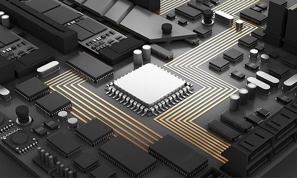
Delivering AI-Powered Spec-to-Platform Solutions for Faster Time to Market
The collaboration signifies a major step forward in enabling AI/ML, 5G, IoT/Edge and automotive innovation built on advanced Arm architectures such as Cortex, Neoverse and Mali. Our joint capabilities support startups across the full semiconductor lifecycle—from RTL design to production silicon, driving custom silicon design and platform optimization for data center, cloud and embedded systems, ensuring high performance and energy efficiency across digital workloads.

Design services
Our semiconductor design services cover product architecture, microarchitecture, RTL design and design verification — ensuring efficient and reliable hardware implementations.
Package design services
We offer routability feasibility analysis, PLOC definition, bonding diagrams and substrate layouts to optimize performance in semiconductor production.

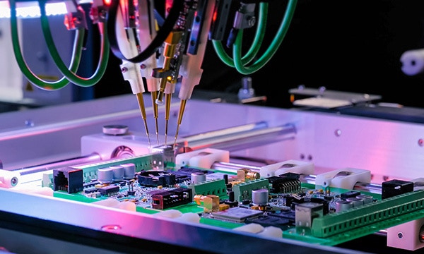
Test manufacturing services
Our services include memory BIST, wafer sort testing, probe card and load board design, yield monitoring and test program optimization.

Semiconductor validation services
We provide essential testing and verification for semiconductor technologies — including pre-silicon validation, process corner characterization, wake-up and functional validation and volume validation.

Qualification services
We ensure thorough testing for packaging solutions with temperature cycling, HTSL, UHAST and HTOL qualification. Our team handles design reviews, fabrication and socket solutions for burn-in boards and burn-in vector development.
Manufacturing services
Our manufacturing services span prototype and risk production — setting up manufacturing flows and creating bills of materials (BOM). Volume manufacturing focuses on supplier management, material monitoring and ongoing quality assurance.
Join Us in Bengaluru
Be part of an exclusive semiconductor startup conversation on accelerating innovation from idea to silicon.
Limited seats. Startup founders, CTOs and silicon architects only.