
Overview
India's semiconductor startup ecosystem has no shortage of talent, capital or ideas. The missing link is access to the ecosystem — the architecture, foundry and engineering partners who move a founder's vision forward.
We hosted our Semiconductor Startup Dinner on June 25 in Bengaluru with Arm and Samsung Foundry, bringing together 30+ semiconductor founders, architects and industry leaders building at the edge of custom silicon.
The evening was built around one question:
What does it take to move from idea to production silicon and accelerate semiconductor innovation?
Discussions focused on the industry's biggest challenges — from reducing risk and driving capital efficiency to tape-out readiness, packaging realities and qualification requirements.

Exclusive Walkthrough: Advanced Semiconductor Lab, Bengaluru
Founders received a private tour of HCLTech’s 40,000 sq. ft. Advanced Semiconductor Lab, which brings the post-silicon workflow together — from working prototype to production-ready silicon. The visit showcased electrical validation, ATE testing, AEC-Q100 and JEDEC JESD22 qualification, failure analysis, in-house surface-mount technology (SMT) assembly and next-generation cooling technologies for AI and high-performance computing.
Capability highlights:
- Class 1K and 10K cleanrooms, with 24/7 secure VPN access
- Full reliability suite, including HTOL, HAST, ESD, temperature cycling and latch-up
- Advanced failure analysis, including SEM, FIB circuit edit, 3D X-ray, Micro CT, CSAM and wafer micro-probing
- In-house SMT line with vacuum reflow, 3D inspection and flying probe
- ISO/IEC 17025 accredition
Inside the Semiconductor Startup Dinner
Explore highlights from an evening of conversations, insights and ecosystem collaboration.


Speakers
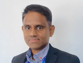
Global Delivery Head, Semiconductor Business, HCLTech
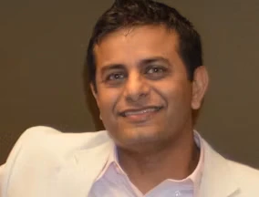
Sales Head, Global Semiconductor Chip Business, HCLTech
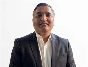
Sales Head, Semiconductor Business, HCLTech India
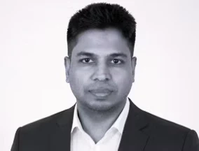
Regional Sales Manager, Arm India and Middle East
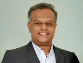
Senior Vice President and Head, Design Platform Engineering, Samsung Foundry
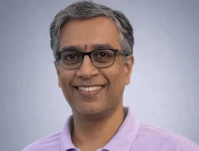
Co-Founder, Agrani Labs
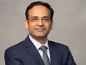
CEO, MOSArt Labs
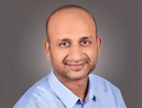
VP SoC Engineering, HrdWyr
General Partner, Speciale Invest
What’s Next
Building on this event, we're looking forward to many more interactions with the startup ecosystem. More conversations like this to come.

Find what inspires and drives you