


From Product Spec to Production Silicon
Custom silicon is now a competitive moat — for hyperscalers, automotive OEMs, industrial players and device makers alike. Getting from product specification to production-ready parts demands tight, coordinated execution across architecture, design, verification, prototyping, validation, qualification and manufacturing where most organizations can't staff every stage.
We take single-point ownership of that journey. Our Spec-to-Parts model spans front-end and back-end design, FPGA and emulation, pre- and post-silicon validation, package design, manufacturing test and qualifications delivered through our in-house labs, 40+ IP partnerships and distinguished relationships with the world's leading foundries.
More than half of our client designs now carry an AI component, from ultra-edge inference silicon to hyperscale training accelerators.
Tape-outs across foundries and nodes
First-silicon success rate
To 2nm-class node experience, including Intel 18A and 14A
Of the top 10 chip companies served
IP vendor partnerships
Our Capabilities
The Complete Silicon Lifecycle, Under One Engineering Roof


Key Differentiators
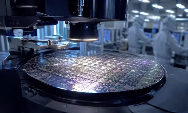
Turnkey silicon across nodes and fabs
180nm to 2nm-class, including ultra-low-power, large-die and multi-die SoC programs with automotive compliance
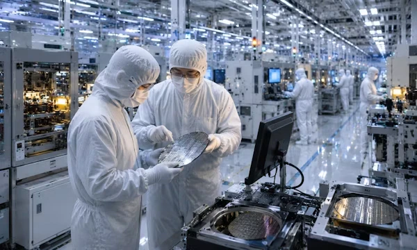
The industry's broadest foundry access
Distinguished design partnerships with TSMC, Samsung, Intel, GlobalFoundries and Rapidus, plus 40+ IP vendor partnerships
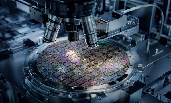
Platform ecosystem
Custom SDV solutions with Intel; Arm Neoverse-based custom SoC solutions as an Arm Total Design partner
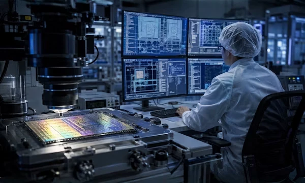
Proven delivery
230+ tape-outs, 95% first-silicon success, world-class validation and qualification labs
Featured: Advanced Semiconductor Lab (ASL)
From first silicon to production readiness — under one roof
Getting silicon to production is harder than it should be, validation in one lab, qualification in another, failure analysis somewhere else — every handoff adds delay and risk.
Our Advanced Semiconductor Lab (ASL) in Bengaluru brings the entire post-silicon workflow under unified engineering ownership, with a 40,000 sq. ft. purpose-built, ISO/IEC 17025 accredited facility, Class 1K and 10K cleanrooms and 24/7 secure VPN access.
Supporting labs:
Silicon tester and validation labs · RF/mmWave lab · high-speed lab (55G EE / 100G optical) · emulation infrastructure · 25,000+ sq. ft. Class 10K ATE cleanroom.


Trends and Insights
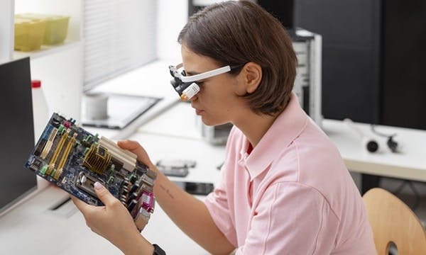
The dawn of AI chips: Pioneering the future of smart technology
AI chips are crucial for technological advancements, enhancing efficiency across industries, but manufacturers are facing challenges due to technical, political and environmental constraints

The future trends shaping the semiconductor industry
In the first episode of the Chip Chat podcast series, Ameer Saithu, Executive Vice President, Semiconductor Business at HCLTech, explores the dynamic landscape of the semiconductor industry, the key drivers for its growth and how emerging technologies are poised to redefine the future of this sector

The AI revolution: How semiconductors are fueling innovation
In this Chip Chat podcast episode, hosted by HCLTech Trends and Insights, Nick Ismail and Biswadeep Chatterjee explore how AI revolution is fueling the growth of AI chips and innovation
Testimonials

Frequently Asked Questions
Absolutely. We have the expertise and resources to take full ownership of the chip design process, from product specification through to tapeout and qualification. Our “Spec to Platform” approach covers front-end and back-end design, validation, prototyping and manufacturing, delivering turnkey semiconductor services and solutions with accountability at every stage.
Our Spec-to-Parts model provides single-point ownership of the entire silicon journey — from product specification through architecture, design, verification, prototyping, validation, qualification and manufacturing — delivered through our in-house labs, IP partnerships and foundry relationships.
Our flagship facility is the Advanced Semiconductor Lab in Bengaluru. It is a 40,000 sq. ft. facility with Class 1K and 10K cleanrooms, AEC-Q100 and JEDEC JESD22 qualification and a full failure analysis suite. All services operate under a single engineering team, ensuring continuity and accountability.
We work across nodes from 180nm to 2nm-class, including Intel 18A and 14A. We maintain distinguished design partnerships with TSMC, Samsung, Intel, GlobalFoundries and Rapidus, plus 40+ IP vendor partnerships.
We use GenAI across the silicon lifecycle through HCLTech AI Force.Semi, HCLTech AI Force.Test and HCLTech AI Force.Embedded — generating test plans, UVM testbenches, assertions, validation code and ATE test programs. This delivers up to 35% productivity improvement and ~25% schedule reduction.
Yes. We deliver ISO 26262 and AEC-Q100 compliant automotive silicon, including full qualification testing — HTOL, HAST, temperature cycling, ESD and latch-up — with integrated failure analysis.