


Overview
The semiconductor industry is entering a defining phase of growth, driven by AI, next-generation computing, advanced packaging and the expansion of manufacturing capacity. SEMICON West 2026 brings together the global microelectronics ecosystem to address these priorities while advancing smart manufacturing, supply chain resilience, sustainability and workforce development.
At HCLTech, we bring more than 30 years of semiconductor heritage, with end-to-end engineering capabilities spanning chip design, equipment engineering, manufacturing and lifecycle services. Our Spec-to-Platform model connects product specification, design, verification, advanced packaging, production testing and post-silicon qualification, helping semiconductor enterprises accelerate development and achieve first-time-right outcomes.
Through Chip2Intelligence, HCLTech combines deep semiconductor engineering expertise with AI-powered platforms and intelligent automation. We work with 8 of the top 10 semiconductor equipment OEMs, 8 of the top 10 chip companies and hold approved SoC partner status with all top four global foundries. Meet us at SEMICON West 2026 to explore how HCLTech is enabling faster innovation, smarter manufacturing and connected engineering across the semiconductor value chain.
Focus Areas
HCLTech's Spec-to-Platform model covers the complete silicon journey from initial product specification and architecture through front-end and back-end design, FPGA emulation, pre-silicon validation, advanced packaging, production testing and post-silicon qualification. One integrated team owns outcomes from the first RTL line to production-ready silicon, eliminating handoff risk and delivering the IP continuity that fragmented engagement models cannot provide. HCLTech is the only semiconductor engineering SI that bridges chip and equipment, design and manufacturing, new product development and installed base optimization.
HCLTech brings a unified engineering model spanning silicon, parts, platforms and manufacturing. Our Spec-to-Platform approach enables customers to engage a single engineering partner across the entire semiconductor lifecycle, reducing complexity and accelerating outcomes.
Key Highlights
- Spec-to-Silicon, Parts and Platform solutions with a proven track record
- Manufacturing enablement, fab operations and yield optimization
- NPD to lifecycle ownership for equipment platforms
Artificial Intelligence is reshaping semiconductor engineering, manufacturing and operations. HCLTech embeds AI throughout the semiconductor value chain, enabling faster design cycles, greater automation and improved engineering productivity.
Key Highlights
- 30% cycle time reduction across the silicon development lifecycle
- Intelligent equipment software engineering and platform automation
- Auto test flow generation for post-silicon and manufacturing test
- €19M Investment in Advanced Semiconductor Engineering Infrastructure
- 40,000 sq. ft. Advanced Semiconductor Lab for Post-Silicon Validation & Testing
- Scalable Engineering Excellence Across the Globe
- 10+ dedicated labs worldwide, including a GenAI Lab in Singapore
- 60+ customer equipment platforms operational
Solutions


Why HCLTech
Semi Engineering SI — Leading design-services player with over 30 years of unbroken semiconductor heritage
SI with Top 4 Fab SoC Partner Status — Approved SoC partner at Intel, Samsung, TSMC and GlobalFoundries with privileged PDK access
Year Relationships — Driving transformation for all of the top 5 Equipment Companies, 8 of the top 10 Chip companies and 3 of the top 4 ISVs
Engineers driving R&D breakthroughs
Tapeouts across multiple foundries and process nodes
First Silicon Success Rate
Highest Investments — Customer Labs, 10k Clean Rooms, Solution Frameworks
Chip-to-Cloud, Spec-to-Platform — the only SI that bridges chip design and equipment engineering with proprietary solution frameworks
Client Testimonials
Our Leaders at Semicon West
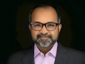
Executive Vice President and Head, Global Semiconductor Business
HCLTech
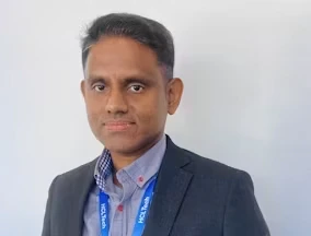
Global Delivery Head, Semiconductor Business
HCLTech
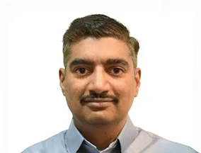
Senior Vice President, Global Semiconductor and OEM Segment
HCLTech
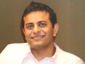
Sales Head, Global Semiconductor Chip Business
HCLTech
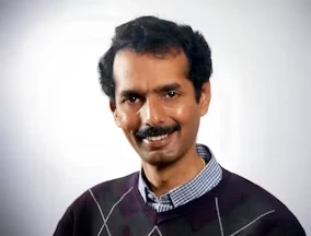
Senior Vice President- Semi Sales
HCLTech
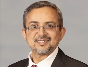
Client portfolio Leader- Semi Sales
HCLTech
